

Simple or highly complex PCB design. Convergence can help you during the development process
- Mar 21, 2024
- 3 min read
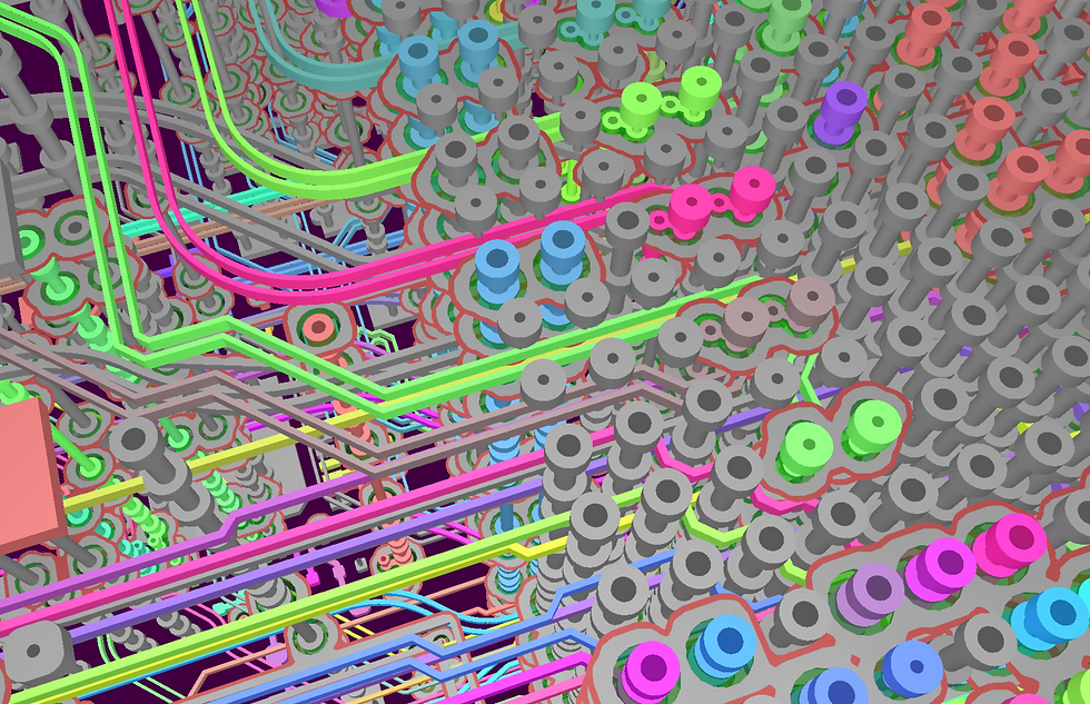
Did you know that Convergence Design Services engineers are working on some of the most complex PCB technology / density? Check out a current design/SI analysis being performed on 28 layer advanced PCB with multiple DDR5 (64bit) and countless PCIeGen5 interfaces.
Designing a Printed Circuit Board (PCB) involves a set of guidelines to ensure the board functions correctly and reliably. Here are some key guidelines to consider:
Component Placement: Place components strategically to minimize trace lengths, reduce noise coupling, and optimize signal integrity. Group related components together to simplify routing. When creating schematics, we always recommend adding notes for anything critical for the layout designer to easily identify.
Routing: Route critical signals first, such as clock lines and high-speed data lines. Maintain signal integrity by avoiding sharp corners, minimizing trace lengths, and ensuring proper impedance matching. Work early and often with your PCB board shop to finalize stack up/via structure / impedances. Back-drilling or micro vias should be utilized for high speed tracks if PCB routing between layers is required.
Trace Width and Spacing: Determine trace width and spacing based on the current carrying capacity and the dielectric material used. Use wider traces for higher currents and maintain appropriate spacing to prevent signal interference. Constrain files can help ensure not potential missed net categorization.
Ground Planes: Incorporate ground planes to provide a low-impedance return path for signals, reduce EMI, and improve signal integrity. Ensure proper grounding techniques, such as stitching vias and connecting ground planes to the chassis or earth ground.
Power Distribution: Design robust power distribution networks to ensure stable voltage levels and minimize voltage drops. Use multiple power planes or dedicated power rails for different voltage levels and sensitive components. On complex or tight tolerance boards we always recommend we run a Power Integrity Simulation
Thermal Management: Consider thermal dissipation requirements and incorporate features such as thermal vias, heatsinks, and copper pours to efficiently dissipate heat from high-power components. On higher power / Mil/Aero advanced thermal simulation is a must!
Signal Integrity: Analyze signal integrity issues such as reflections, crosstalk, and impedance mismatches using simulation tools. Implement controlled impedance traces for high-speed signals to maintain signal integrity. In instances of very high speed tracking or data alignment advanced Si with Hyperlynx is recommend.
Design for Manufacturing (DFM): Follow DFM guidelines to ensure the PCB can be manufactured efficiently and reliably. Consider factors such as minimum trace widths, annular ring sizes, and solder mask clearances.
Design for Assembly (DFA): Optimize the PCB layout for ease of assembly, including component orientation, access for soldering, and minimizing the use of vias under surface-mount components.
Electromagnetic Compatibility (EMC): Mitigate electromagnetic interference (EMI) by carefully routing signal traces, incorporating shielding where necessary, and adhering to EMC standards and regulations. For space or Mil/Aero we recommend an EMI analysis on SCH/PCB design to ensure best path at success. This coupled with our onsite EMI chamber for prequalification testing allows for a smooth formal qualification process.
Testability: Include test points and access for probes to facilitate testing and debugging during production and maintenance. Volume dependent for ICT vs FP
Documentation: Maintain thorough documentation including schematics, layout files, bill of materials (BOM), and assembly drawings to aid in manufacturing, testing, and troubleshooting.
Environmental Considerations: Consider environmental factors such as temperature, humidity, and vibration when selecting materials and designing the PCB layout. Conformal coating, enclosure design, vibration, thermal, dust/water ingress etc are all key factors for environmental considerations in rugged environments like DO-160 or MIL-STD requirements.
Feel free to reach out to your design experts at Convergence Design Services for any guidance or other tips/tricks of the PCB design process.


